
- TOP
- Cutting-edge Research and Social Contribution
- Cutting-edge Research
- Flexible transparent electronics realized with oxide semiconductors
Flexible transparent electronics realized with oxide semiconductors
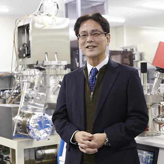
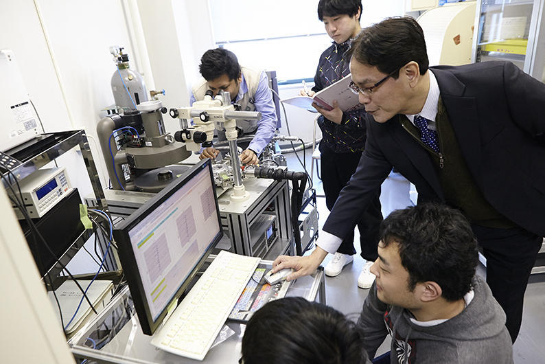
FURUTA Mamoru
- Specialized field
electrical and physical properties of semiconductor materials, semiconductor processes and device technology, thin film transistors, flat panel displays
Development of high performance thin film transistors for next generation displays
Thin film displays are widely deployed in televisions, personal computers and smart phones. In recent years, high definition technology has advanced dramatically. Current high-vision broadcasting on television uses images of approximately two million pixels, but Super Hi-vision broadcasting, which NHK aims to implement by 2020, has 16 times that number of pixels. Professor Furuta says, "It seems that broadcasting technology has changed greatly in the past five years, in terms of its ability to recreate highly realistic impressions by means of super high definition."
Currently, most thin film displays are controlled with silicon-based thin film transistor technologies, but some problems have arisen related to advances in ultrahigh definition large screen displays.
Prof. Furuta explains, "The displays of personal computers and mobile phones are arrays of a very large number of primary color (red, green, and blue) elements called fine pixels. Extremely small transistors contained in each pixel control the way the pixels radiate light, but lately it is being said that the base material, silicon, is about to reach the limit of its capacity. That is, silicon exhibits high performance in a crystalline state where atoms are arranged regularly, but if the arrangement of the atoms is disturbed, performance degrades immediately. At present, there is no technology for using crystalline silicon in the fabrication of large size devices such as displays, so there is no choice but to continue using amorphous silicon, whose atoms are randomly arranged. With amorphous silicon, performance is just one thousandth of that using crystalline silicon."
In other words, with silicon transistors it is difficult to maintain performance and at the same time enlarge display area, so there is a need for materials with higher performance. As a result, recently attention has been drawn to oxide semiconductors, which can be deployed in large area devices while maintaining high performance. These new semiconductors are said to be capable of at least 10 times better performance than that of amorphous silicon ones. Prof. Furuta has been conducting research on the use of oxide semiconductors in thin film transistors for next generation displays.
In 2005 Prof. Furuta's research group succeeded in the world-first accomplishment of displaying images in a liquid crystal display using a zinc oxide based oxide semiconductor transistor. The group's success was highly evaluated worldwide.
Prof. Furuta adds, "In 2006, we presented this outcome at an international display technology conference in the US. Out of about 500 presentations there were only three presentations concerning the use of oxide transistors. However, currently the number of presentations on this topic is more than half the number of presentations of that academic society. Clearly, not only the academic world but also the industrial world is paying significant attention to this technology."
At present Prof. Furuta is developing those research outcomes further and is conducting collaborative research with companies to refine the characteristics of the materials and improve their device performance and reliability.
"In order to industrialize new materials, those materials must have the desired properties, but they must also be reliable and safe, and there must be technology for controlling them. With all those issues in mind, I am conducting research as a link between industry and academia," says Prof. Furuta.
Prof. Furuta, who used to work for a major home appliance manufacturer and has considerable experience with the process of developing new technology, disseminating it to society and achieving its mass production (i.e. moving from research and development to commercialization to the construction of mass production factories). The broad vision he acquired there has become the basis of his research life.
High resolution image sensors: Utilizing the transparency of oxide semiconductors
Prof. Furuta is also focusing on the application of this technology to new fields by taking advantage of oxide semiconductors' transparency to visible light. As a part of that work, in collaboration with Science and Technical Research Laboratories (NHK STRL), he and his team have developed a new image sensor that contributes to the miniaturization of Super Hi-Vision cameras.
In order to obtain high quality color images with the current trial-basis Super Hi-Vision cameras, color separation optics are widely used in the separation of incident light into the three primary colors, blue, green and red, and capturing them with three separate imaging devices. However, this system can only be downsized so much. On the other hand, single image sensors with color filtering can achieve more compact camera size than three-sensor devices. There is a drawback to single image sensors, though: only one third of incident light can be converted into signal. Furthermore, when pixel density increases, the light detection area for each pixel becomes small and the amount of incoming light decreases, which gives rise to the problem that a clear image cannot be captured under low light conditions. In other words, in order to capture high sensitivity, high definition images, the efficiency of conversion of the incoming light is very important.
On the other hand, current single sensor color imaging devices are in principle inferior to three sensor type devices in terms of sensitivity and resolution, and thus are not suitable for Super Hi-Vision cameras, which require high image quality.
To overcome these problems, it is conceivable to use a stack of three single plate color imaging devices. This would separate incident light into the three primary colors in the depth direction without color separation optics, and theoretically that would make it possible to convert 100% of incident light.
Prof. Furuta explains, "This method was proposed a long time ago, but it has not been realized yet. The problem is that each individual sensor requires a signal readout circuit for external extraction of the absorbed light as an electrical signal. Since conventional silicon-based circuits are non-transparent in visible light, the light cannot penetrate downward."
So far no one has created a transparent circuit, i.e. one that combines electrical functionality and the capacity to allow light to pass through to a lower layer.'
Prof. Furuta continues, "Since silicon transistors are not transparent to visual light, the light does not reach the bottom of the devices. Then I thought if I used transparent materials to create a circuit that could read signals, that transparent circuit could read the information about how much photoelectric conversion had been done in that layer and allow the incoming light to pass through to the next layer."
He and his team fabricated an image sensor consisting of a laminate of three cells. Each cell contains an organic photoelectric conversion film (with a transparent signal readout circuit) which is sensitive to only red, green or blue light. The team realized an image sensor that performs color separation by absorbing in turn the three colors of light passing depthwise, and successfully achieved color imaging without color separation optics. The miniaturization of the Super Hi-Vision camera became a reality with this single advance: the successful development of a stacked image sensor with transparent signal readout circuit.
The potential of transparent electronics to change our lives
Currently, Prof. Furuta has begun work on the development of 'transparent ambient electronics' which do not feel like they contain functional materials. In his work to develop an invisible circuit consisting of a functional oxide semiconductor on a transparent substrate such as glass, his ideas are steadily expanding to realize unprecedented functional devices such as transparent displays and transparent ID tags which display information only when required.
Prof. Furuta says, "By incorporating a transparent circuit in glass such as a window, various devices such as display sensors and transparent solar cells can be incorporated in glass. Likewise, a ubiquitous environment in which information can be provided anywhere in the surroundings would be a dream no longer."
Now Prof. Furuta is setting his sights on the possibility of flexible electronics using transparent and elastic substrates such as plastics and films, for application in the medical and health fields, in devices such as wearable sensors that monitor human health, and contact lenses with artificial retinal functionality thanks to the use of high definition image sensors.
"By giving a degree of freedom to device shape, it will be possible to expand the range of applications. Since these devices are invisible, people will not be conscious of the fact that they are wearing them or even that they exist. I believe that it is possible now to create many new applications to support our daily life, and that before long a new future will likely open up for electronics."
Transparent electronics open the door to a new future that could not be created before. It seems this will improve our lives significantly.