
- TOP
- Cutting-edge Research and Social Contribution
- Cutting-edge Research
- Developing ultimate nanodevices through the understanding of a "single atom"
Developing ultimate nanodevices through the understanding of a "single atom"
INAMI Eiichi
- Specialized field
Nano-functional-materials/devices, Scanning probe microscopy, Single Atom/molecule manipulation, Optical Properties of Materials, surfaces/interfaces
Tiny particles called atoms make up everything around us. Air, water, and the human body all consist of these atoms. About 40 years ago, a revolutionary microscope was invented that could not only visualize atoms, which are invisible to the naked eye, but also manipulate them individually. This was the Scanning Probe Microscope (SPM). Professor Eiichi Inami is exploring the microscopic world using this specialized microscope as his key instrument, taking on the challenge of developing nanomaterials that could lead to innovations.
Atomic-level manufacturing to further advance microfabrication technology
From smartphones and electric vehicles to digital appliances, financial systems, and transportation infrastructure...Semiconductors serve as the key component driving the rapid advancement of digitalization. Professor Inami explains, "Through the dramatic evolution of semiconductor microfabrication technology, we have achieved higher performance, miniaturization, and improved energy efficiency across all systems." Smartphones are a prime example of this trend. The latest iPhone model contains 19 billion transistors. In other words, an incredible number of semiconductor components--so tiny that they are invisible to the naked eye--are densely packed into a device small enough to fit in the palm of your hand.
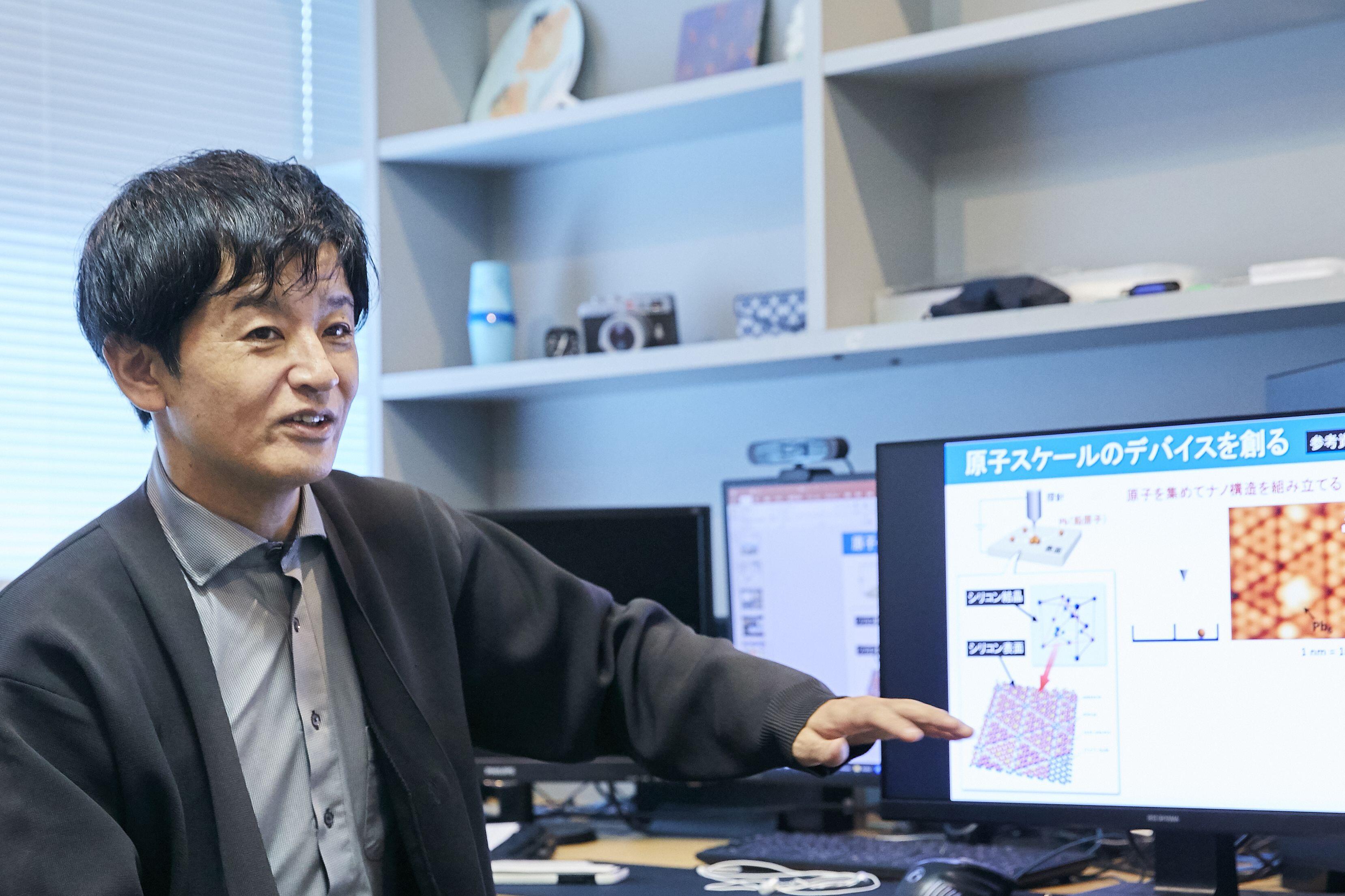
"Atomic manipulation"--i.e., observing and moving individual atoms using a scanning probe microscope (SPM)*--holds great promise as a novel approach based on this principle to meet the growing demand for technological innovation. Professor Inami is working to advance this cutting-edge microfabrication technology. Using SPM, researchers are gaining deeper insights into material structures and properties at the single-atom level. This research not only enables the discovery of new material characteristics and functions but also facilitates the development of technologies that allow precise control over these properties.
*A microscope that can measure the shape and physical properties of a sample's surface at the atomic scale by tracing it with a sharp needle (probe) featuring a single atom at its tip. Unlike an optical microscope, it does not rely on lenses but instead consists of precision machinery and a monitor.
Unveiling still-unknown atomic properties to drive the development of ultra-high-performance devices
Professor Inami has made numerous globally impactful discoveries through his previous research using SPM. One such breakthrough is the finding that when a small amount of visible light is shone on graphite, which consists of carbon atoms, part of it transforms into a material (called diaphite), exhibiting properties intermediate between diamond and graphite. While carefully investigating this phenomenon, he successfully became the first in the world to directly observe, at the atomic scale, a photo-induced phase transition--a process in which a material's structure and properties change upon exposure to light--and elucidated its underlying mechanism. Furthermore, he discovered that the phase transition process varies significantly depending on the wavelength of light, demonstrating that light tuning enables atomic-level control over the transition. These findings are expected to accelerate the development of new materials.
Nanoclusters--aggregates of multiple atoms--are known to exhibit dramatic changes in their properties depending on the number of constituent atoms. Professor Inami states that he and his team made a significant discovery while diligently conducting experiments to uncover hidden properties by precisely controlling the size of these nanoclusters at the single-atom level.
If a method can be developed to arrange these clusters at high density and reliably induce switching, it could pave the way for ultra-high-performance computers and devices.
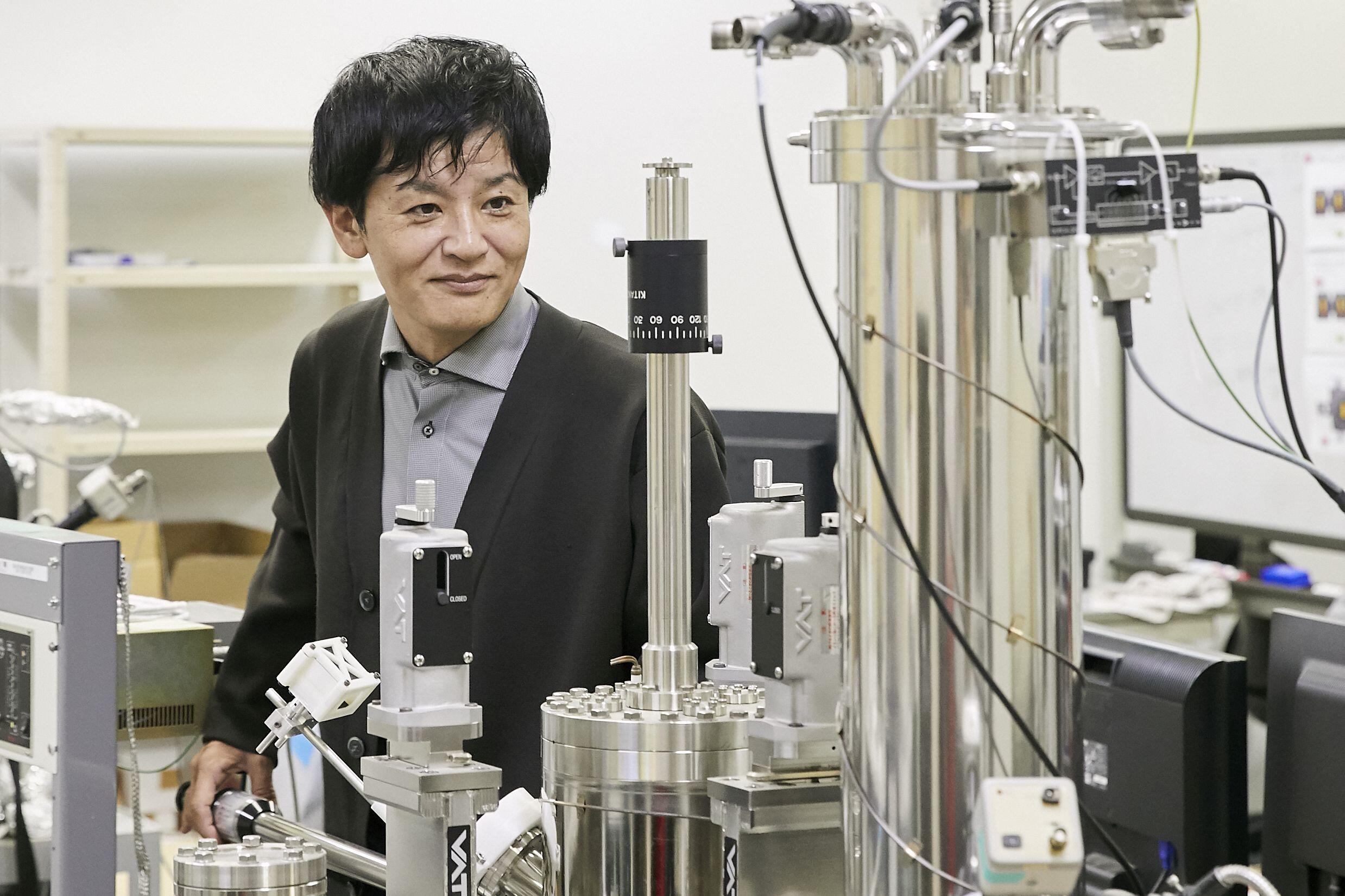
Recently, he has been actively working on the development of new SPM-based devices. More than 40 years have passed since SPM was first developed at IBM's Zurich Research Laboratory in Switzerland, and performance improvements are now essential to keep pace with advancements in microfabrication technology. To address this, Professor Inami and his colleagues have devised a microscopy technique utilizing the pulsed voltage method. Pulsed voltage refers to a voltage waveform that rises sharply, remains for a short duration, and then drops sharply. His team is developing a novel approach that enables surface observation while applying a series of such pulses to the sample.
Expectations are growing for technological innovations that will further advance microfabrication technology.
Aiming to pioneer a new field through the combination of light and atomic manipulation
Professor Inami is currently working on atomic-scale manufacturing, utilizing a wide range of techniques such as material analysis, processing, and equipment development. However, his fascination with the microscopic world began when he was in junior high school.
He went on to study in the Faculty of Science at university. By analyzing material structures using methods such as X-ray analysis, he intellectually understood the atomic structures. However, his desire "to see atoms directly with his own eyes" only grew stronger. Then, the long-awaited moment arrived.
Although he specialized in astrophysics as an undergraduate and studied the optical properties of materials during his master's program, this experience led him to pursue atomic manipulation using SPM. Since then, he has been working on a wide range of research themes, from microscopic to macroscopic, using SPM as his key research tool. In 2018, he joined Kochi University of Technology to establish his unique research approach, integrating all of his previous experiences.
Currently, he collaborates with other universities on cutting-edge research, while also working with KUT faculty members in information science to integrate AI into theoretical calculations that predict material properties from atomic structures. Through this approach, he is developing technology to predict various functions more quickly and accurately. At the core of his ambition lies a consistent goal: "I want to create unprecedented new devices by freely combining atoms."
Date of posting: February, 2025/ Date of interview: November, 2024