
- TOP
- Cutting-edge Research and Social Contribution
- Cutting-edge Research
- Realizing high-efficiency energy devices using nanomaterials to solve local and global issues
Realizing high-efficiency energy devices using nanomaterials to solve local and global issues
FURUTA Hiroshi
- Specialized field
Thin Film Technology, Nano-materials, Condensed Matter Physics, Applied Optics/Quantum Optics, Energy devices (Electricity generation, storage, conversion), Metamaterial
Bringing out new properties of light through nanoscale circuit design
Recent progress of nanotechnologies in terms of observation techniques and fabrication processes allows us to access novel electric and photonic properties of nanomaterials, and those properties are derived directly from their size and the structure of their matter. Among nanomaterials, nanocarbon materials--exemplified by carbon nanotubes and graphene--are one of the materials attracting the most attention in the nanotechnology field. In addition to their large surface area relative to their size, their electrical conductivity, thermal conductivity, mechanical strength, and other properties have been shown to exceed those of existing materials significantly. They are expected to be applied as electronic, optical, and energy materials.
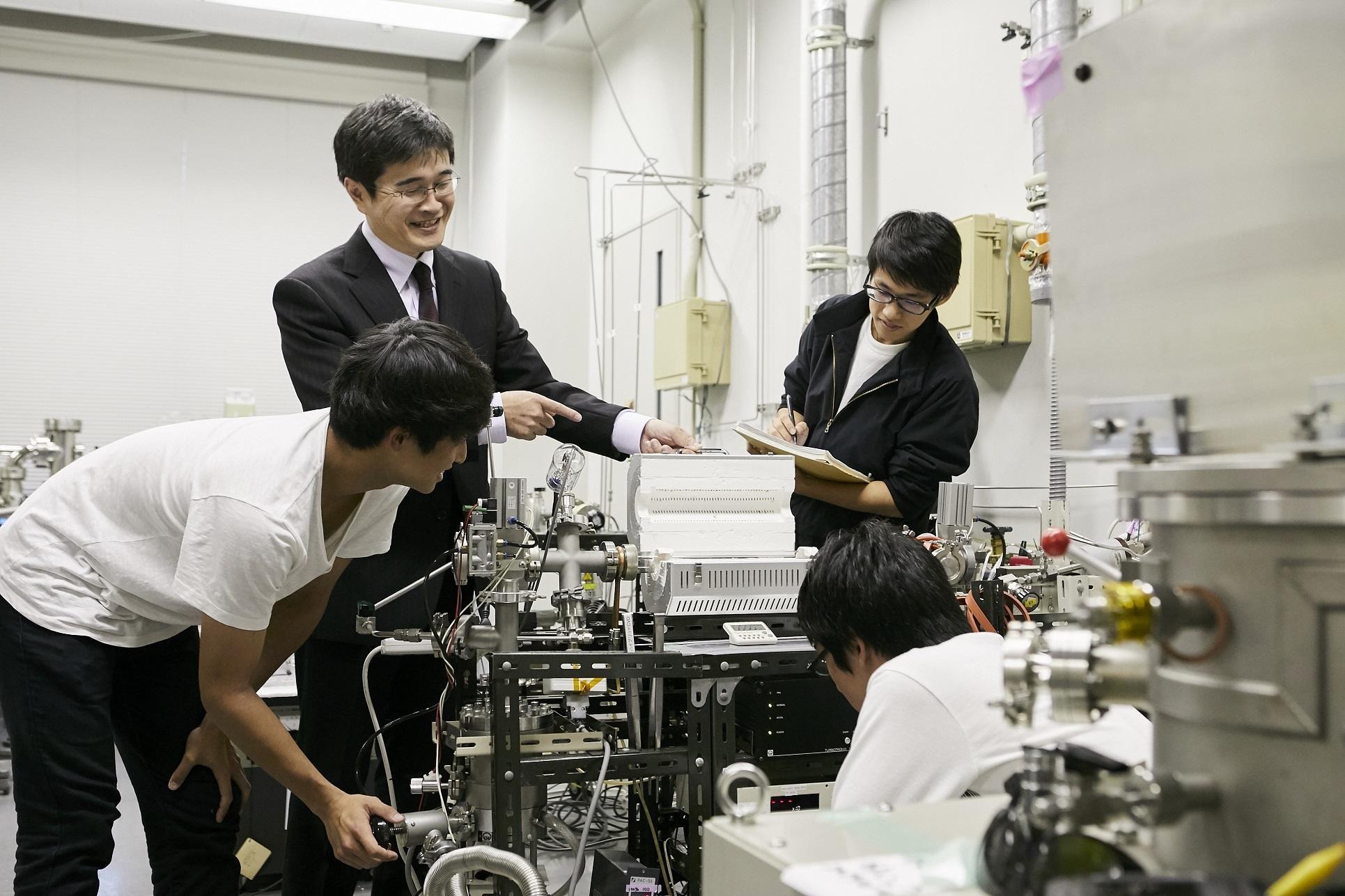
Professor Hiroshi Furuta has conducted research on structure control of carbon nanotubes and other nanomaterials and applied these nanotubes to applications in energy devices such as electrodes for dye-sensitized solar cells, heat spreader and solar collector materials, and electron emission source materials. In particular, he is focusing efforts on applications in the field of optics using the principle of "metamaterials."
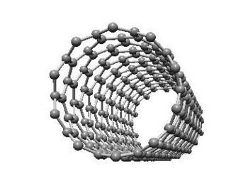
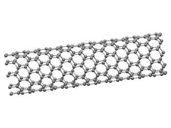
(Carbon nanotubes, nanometer-sized concentric cylindrical carbon structures made of graphene)
Metamaterials are artificial structures, such as electrodes, designed on a scale larger than atoms and molecules, and smaller than electromagnetic waves, and they exhibit physical properties and functions that are impossible to achieve with natural materials.
Carbon nanotubes, which have outstanding electrical and optical characteristics, are promising as a component material of metamaterials to realize ultra-small optical devices.
One of the factors that make carbon nanotubes so promising in metamaterials is that they have a self-organized growth process. Top-down processes have been traditionally used to create nanometer-scale objects, in which small objects are created by reducing the size of large objects. However, as this process is reaching its lower limit of size, attention is now shifting to the idea of using a bottom-up process where functional morphology and physical properties are derived by self-arranging and self-organizing atoms. There is a need for technologies to build up complex structures spontaneously based on intricate circuit designs without relying on artificial manipulation (i.e., "processing").
Carbon nanotubes have a property whereby individual nanotubes spontaneously form structures and grow through a bottom-up process. There is a possibility that the fabrication of delicate and complex structures, which is essential for metamaterial applications, can be achieved by a simple process.
"A carbon nanotube is an electrical wire made up of a graphene sheet curled into a cylindrical form. It has a nano-size diameter that can be controlled in length. Carbon nanotubes can be grown like plants by supplying carbon feed gas to catalyst nanoparticles planted like seeds on a silicon substrate. By using a bottom-up process, it is possible to form wiring in a self-organized manner, and there is a possibility that, in the future, we will be able to form things like circuit wiring patterns on a nanometer scale as intended."
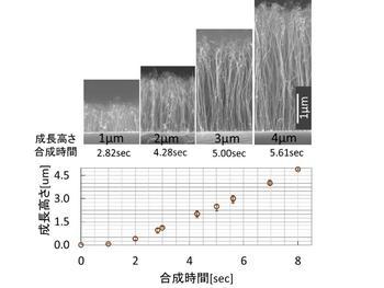
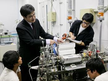
(SEM (Scanning Electron Microscope) images of carbon nanotubes with height precisely controlled by adjusting the synthesis time, and carbon nanotube synthesis equipment assembled with students)
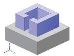
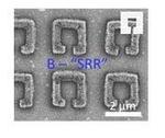
(Internal structure of metamaterial electrodes whose constituent material is carbon nanotube. Light absorption functionality is improved through an intricate circuit design [1])
[1] A. Pander, K. Takano, A. Hatta, M. Nakajima, H. Furuta, Optics Express, 28(1) (2020) pp. 606-625.
"In the field of nanomaterials research, which has been traditionally based on knowledge of chemistry and mechanics, our strength lies in our ability to approach the extraction of optical properties through circuit design. In this situation where energy resources are scarce, conventional techniques such as adding rare elements to bring out specific properties have been adopted to realize high-efficiency electronic and photonic devices. However, it is also possible to build systems with a low environmental impact by performing circuit design and absorbing specific types of light. This is truly a paradigm shift, and we are extremely excited to be able to apply circuit design to material properties."
For Japan, where energy resources are scarce, the ability to use circuit design to bring out new properties of materials will be extremely important.
The design of circuits is one of the areas human beings are good at, but limitations arise when creating designs on a large scale. According to Professor Furuta, "To create nanometer-scale structures on a large scale and make them function, we need to learn from nature." We can see the phenomenon of self-organized pattern formation everywhere in the natural world.
"The surface of the snail's shell is one example. If you look at it with an electron microscope, the surface has nanometer size bumps and indentations, and these have a sophisticated cleaning function. Other functional structures are also formed through self-organizing phenomena in the natural world, such as beautiful snowflakes and quartz crystals. Until now, humans have had to design and build nanometer-scale structures from scratch to achieve a specific function. We have taken a step up from that level. By exploiting things like the process of self-organizing growth, as seen with carbon nanotubes, and creating structures that imitate the self-organization seen in the natural world, we are trying to create new metamaterials which absorb or reflect light, and thereby change color."

Professor Furuta has successfully designed circuits in which nanometer-scale electrodes are formed in a self-organizing fashion. The unique feature of Professor Furuta's research is his desire to learn from the natural world in his optical engineering--attempting to bring out new properties of light by using nanometer-scale circuit design and natural, self-organizing pattern formation.
Proposing a first-in-the-world concept: Applying carbon nanotube forests to metamaterials
A large number of carbon nanotubes aligned perpendicularly to the substrate surface is called a "carbon nanotube forest" because it looks like a forest of trees. Carbon nanotube forests have outstanding optical characteristics for light absorption, not found with any other material.
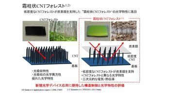
In 2013, Professor Furuta's research group focused on the structure in which a low-density carbon nanotube forest is formed in a self-organizing fashion under a carbon film. They succeeded in controlling the thickness of these structures and discovered their outstanding optical characteristics for the first time. These have a structure similar to the frost columns that exist in nature, and thus are called a "frost column-like carbon nanotube forest."
Fabrication has been demonstrated for "fishnet-type" metamaterials in which minute holes are opened in a regular way in the surface of the carbon film of a frost column-like carbon nanotube forest. Light absorptivity was evaluated, and the results showed that a frost column-like carbon nanotube forest processed into a fishnet form has increased light absorption [2].
"We were surprised to find that, when small holes were made in a carbon film, the light was absorbed instead of passing through. The current generated by the light passing through the holes spirals and absorbs the energy. That sort of antenna-like structure was realized at the nanoscale. Through many experiments and simulations, metamaterials that absorb light are now being realized."
The realization of a frost column-like carbon nanotube forest metamaterial, with a unique hollow structure and a fishnet-type pattern, is expected to broaden the scope of carbon nanotube design and yield applications to new optical devices such as high-precision light detection and optical filters. The results of this research are attracting attention as a first-in-the-world concept using carbon nanotubes in a metamaterial, i.e., a carbon nanotube forest metamaterial.
"Carbon nanotube forest metamaterials are an exciting interdisciplinary field in which remarkable new properties can be created through control using circuit designs. By allowing self-arrangement of carbon, a familiar nanoscale electrode material, it is possible to store the energy of light such as infrared rays, which has previously been thrown away, and recover it as electric power."
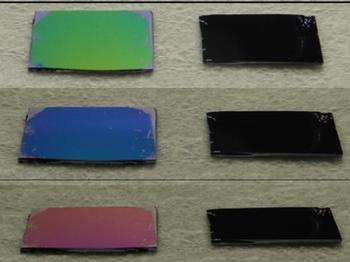
Furthermore, Professor Furuta has found that frost column-like carbon nanotube forests are similar to the structure on the surface of chameleon skin, and he is trying to link this with realization of new properties.
"On the surface of a chameleon's skin, frost column-like crystal structures are arranged periodically, and the color is freely varied by changing the spacing of the skin's nanophotonic crystals with different indices of refraction. Just as the chameleon changes its color by controlling its nano-size structure, we want to create structures with frost column-like carbon nanotube forests where color can be freely varied, like a chameleon, by controlling the distance between the carbon film and substrate."
(At left is a frost column-like carbon nanotube forest, and at right is the conventional-type [2])
[2] H. Miyaji, A. Pander, K. Takano, H. Kohno, A. Hatta, M. Nakajima, H. Furuta, Dia. Rel. Mater. 83 (2018) pp.196-203.
A desire to help solve global energy issues, especially in rural areas and developing countries
As part of his applied research on carbon nanotubes, Professor Furuta has worked with corporate partners to develop an electron emitter boasting a world record of "6 years of stability." This was achieved by using the sharpness and chemical stability of the carbon nanotube tip. This is attracting the attention of various industries, and a search is underway for a way to exploit this as a special field emission electron source that won't be involved in price competition.
In this way, Professor Furuta has demonstrated the potential of carbon nanotubes through basic research, application and development. What sort of future does he want to achieve through these researches? He says, "I want to solve global energy problems using nanomaterials. That's my ultimate goal."
He says his aim is to develop low-cost energy devices with low environmental impact--to help solve energy problems, particularly in rural areas and developing countries, while tackling the major theme of solving global energy problems by applying nanomaterials to high-efficiency energy and communication devices.
"In the near future, we will likely shift from a society where large amounts of energy are produced in one place and then distributed to various locations, to a society of decentralized energy where individuals can manage their own energy. There will be a need for small-scale energy devices that enable individuals to generate and store energy needed for their own use, and convert just the amount needed in each home. Nanomaterials have a large surface area, so they can easily store energy, and efficiently convert light into energy. I'm convinced that, by using nanomaterials, we will be able to achieve development of energy devices at personal and household scale."

With the rapidly progressing trend of a decreasing birthrate and aging population, Kochi Prefecture--with its many depopulated villages full of senior citizens--has the potential to be at the cutting edge of the decentralized energy society. Professor Furuta will make deep inroads in his quest to solve the community-specific and global energy problems that confront us.