- TOP
- Cutting-edge Research and Social Contribution
- Cutting-edge Research
- Foundation technology towards next-generation electronics: Free manipulation of oxide semiconductor characteristics
Foundation technology towards next-generation electronics: Free manipulation of oxide semiconductor characteristics
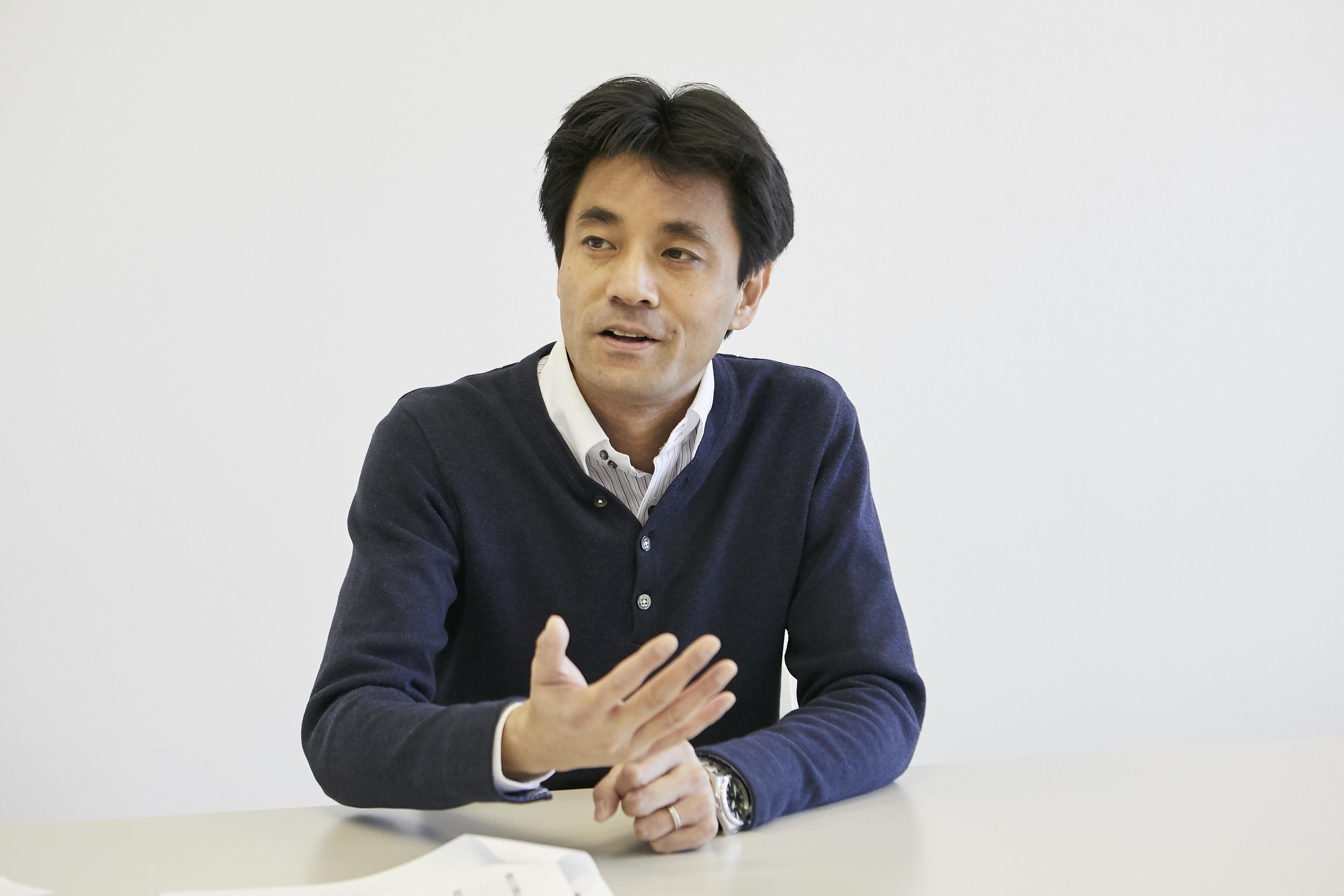
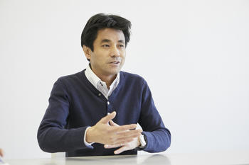
MAKINO Hisao
- Specialized field
solid state physics, physics of semiconductors, thin film technology
Elucidating new properties of materials toward the realization of p-type zinc oxide
Oxide semiconductors are referred to as a treasure chest of functions because of their diverse properties. They have attracted attention as next-generation materials that exceed the performance limits of conventional semiconductors. Since they are transparent and exhibit high conductivity, they are widely used as transparent electrode material for LCD TVs, smartphone displays and solar cells, and have become familiar materials in our daily life.
Professor Makino says, "I think oxide semiconductors are a group of materials with great potential for the creation of new things by combining their various characteristics." When he was a research assistant at Tohoku University, Prof. Makino was working on the development of highly efficient electronic devices that utilize the magnetism of dilute magnetic nitride semiconductors. At one point he asked Professor Tetsuya Yamamoto of KUT (who was then conducting research on semiconductor material design by means of theoretical calculations) to perform some band calculations for him. That request led to joint research between KUT and Tohoku University. As a result of that collaboration, Prof. Makino joined KUT in 2005 as a member of a team promoting industry-academia collaborative research on film formation technology for transparent conductive films using zinc oxide, a representative oxide semiconductor. Since then, with the aim of applying oxide semiconductors to devices to enable new functions, he has been conducting a variety of research, ranging from the development of technology for zinc oxide thin film growth to the elucidation of electronic and surface/interfacial physical properties.
The biggest challenge in the use of zinc oxide as a semiconductor material is the realization of p-type zinc oxide that meets device quality requirements. There are two types of semiconductors, n-type and p-type, and both are required for use in semiconductors. However, zinc oxide tends to be n-type, and it is extremely difficult to create p-type zinc oxide.
Prof. Makino says, "Transparent conductive oxides and transparent electrodes using zinc oxide are both n-type applications, but in order to broaden the applications of oxide semiconductors, the realization of p-type zinc oxide is indispensable. If we can make a high-quality p-n junction, the range of applications will expand immediately. Then we could say for the first time that zinc oxide has joined the ranks of semiconductors."
In order to realize p-type zinc oxide, the key is to understand the essential properties of the material and find means of achieving new properties.
Pursuing complex and unexplained physical properties of polycrystalline materials
There are two types of semiconductors, single crystal and polycrystal. Most crystalline solid materials made of polycrystals consisting of what we call a plurality of single crystals. Prof. Makino is also pursuing research toward zinc oxide polycrystals. Since those polycrystals can form a large area of film at a much lower cost than single crystals, polycrystalline thin films are used in advanced electronics such as flexible displays, which are expected to be used widely in the near future.
"Not only can polycrystalline thin films be used for various purposes, they also have great merits in terms of practical considerations, such as low cost film fabrication. In addition, many of the properties of polycrystals have not yet been elucidated, which makes them interesting as research subjects. These materials greatly stimulate my intellectual curiosity."
One phenomenon that is not yet well understood is the "grain boundary" interface between adjacent crystals within polycrystals. Grain boundaries have been characterized as having properties similar to those of the surfaces of crystals.
On a crystal surface, atoms lose their covalent bond partners, and unbonded 'hands' stick out. Under the unstable state when there are electrons without bonding partners, chemical activity becomes high, which greatly affects physical properties such as electron mobility within the crystal. Grain boundaries, which are said to be close to the properties of the crystal surface, have similar properties.
"The grain boundaries between polycrystalline crystals that are packed with 20-30 nm crystals are extremely small, but they interfere with the movement of electrons. Specifically, when oxygen and water in the atmosphere are absorbed at grain boundaries, the flow of electricity is impaired, causing electrons to bounce off or flick off. I am going to persevere step-by-step with my study of this phenomenon to find out the mechanism of that interference."
Furthermore, on a crystal surface, electrical properties arise when gas from the atmosphere, which was adsorbed on the unbonded hands, is removed. Similarly, at grain boundaries, removing adhering matter allows electricity to flow. In addition, the properties of a thin film change dramatically; for example, depending on the presence or absence of adsorbents at the grain boundaries, a semiconductor might glow or not glow. By making innovative use of such characteristics, various applications such as gas sensors become imaginable.
"Since the characteristics and properties of polycrystals are intertwined with numerous complex factors, it is extremely difficult to gain an understanding of those characteristics and properties. Currently very few researchers are pursuing those questions; as a result, many questions remain unanswered, such as why do such characteristics emerge? and how can we improve those characteristics? That is why I have been aiming to identify and elucidate such physical properties with interesting possible applications, and to create new characteristics, while at the same time pursuing the details of what is happening inside the crystal."
What is happening in the micro world? Attempts to uncover the invisible with various experiments.
One achievement of Prof. Makino was his clarification of the properties needed to improve the quality of zinc oxide based transparent conductive films. He discovered that by controlling the atomic arrangement of the crystal structure of zinc oxide polycrystals, it is possible to achieve higher quality transparent conductive films. In other words, through his experimental results, he demonstrated chemical properties that were previously just speculation.
"It has been said that even if the crystals in a polycrystalline body are bent slightly out of alignment, very unwelcome characteristics may appear. With that in mind, if we make full use of film formation technology and neatly arrange the atomic array of crystals, we will be able to improve the properties of transparent conductive film."
These steadily emerging research results will be the foundation for the realization of p-type zinc oxide.
Hoping to spread the latest analytical technology to the industrial world
During the process of forming a film on a glass substrate, what is adsorbed on the surface and what state is it in? How will the film change when it is exposed to the atmosphere after film formation? In order to further explore the physical properties of polycrystalline materials, it is essential to have high-precision evaluation technology integrated into film formation technology.
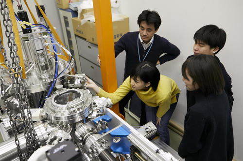
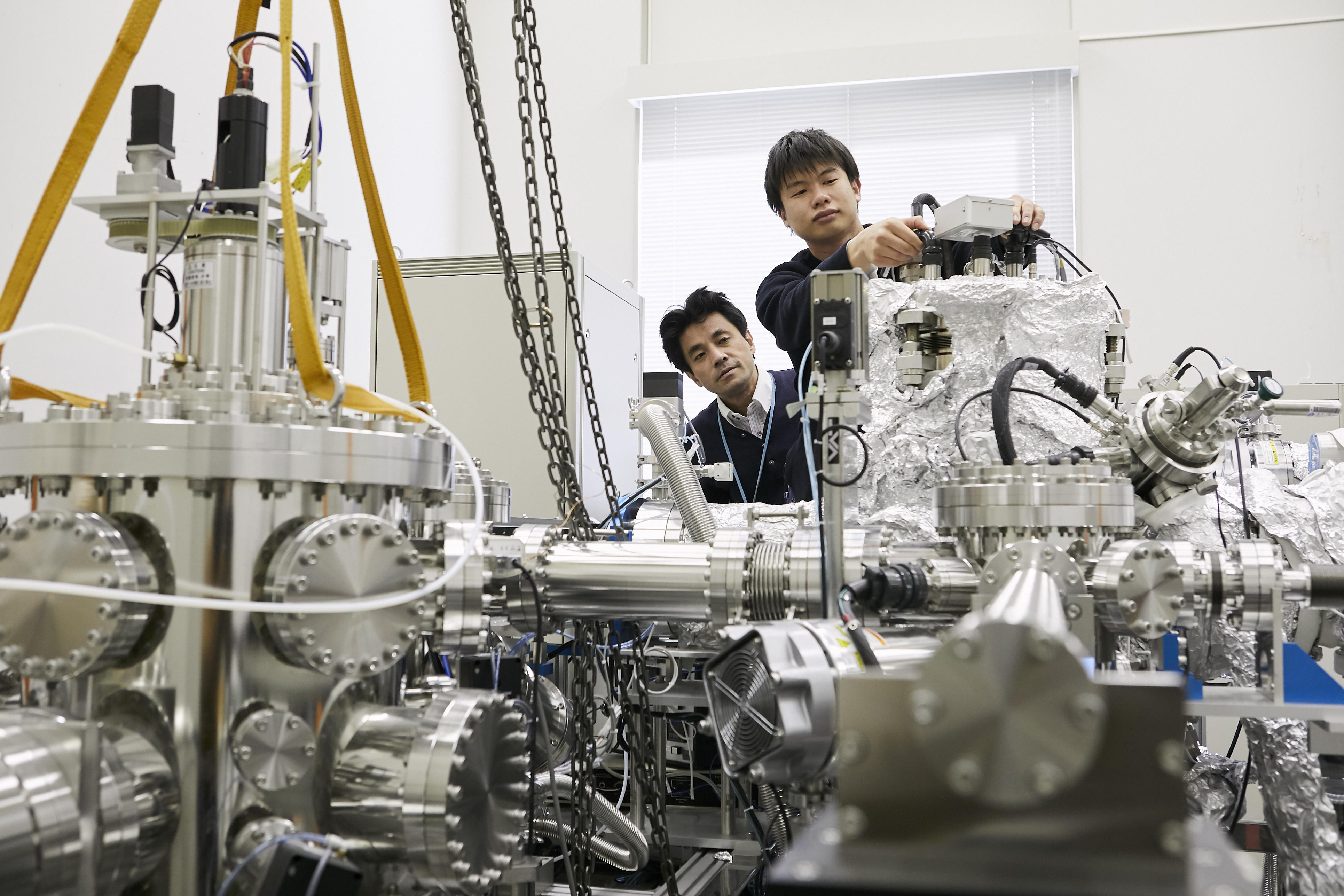
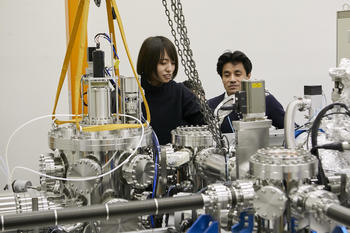
KUT has a double X-ray source Hard X-ray Photoemission Spectroscopy device, one of just a few in the world. It can examine not only the surface of a thin film but also the internal properties slightly below the surface. It is a source of pride to be at the forefront of evaluation technology.
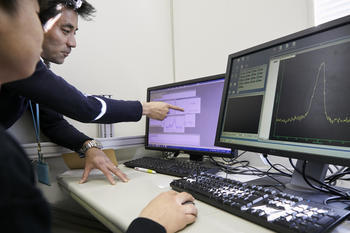
"A double X-ray source Hard X-ray Photoemission Spectroscopy device can emit high-energy X-rays; that allows us to investigate the energy structure of electrons on the surface and in the region just below the surface. When an X-ray strikes matter, some of the electrons pop out; then by measuring the energy of the electrons at that time, we can determine the original state within the film. In that sense, this is a very important experimental technique in the field of material chemistry, enabling us to investigate the state within thin film. We may gain new insights by comparing the state on the surface and the state below the surface."
Moreover, Prof. Makino is developing industry-academia collaborative efforts to enable the wide use in industry of analysis technology based on double X-ray source Hard X-ray Photoemission Spectroscopy.
"With recent analyzers it's becoming easier and easier to measure phenomena at the touch of a button, and get valuable results. Many engineers who made contributions in the dawn of this new age feel a sense of crisis regarding this trend. They are worried that in the future researchers may just accept the results from analyzers, and treat them as data. I think it is necessary to develop young engineers who can understand what is happening inside a substance and correctly interpret to the results. Therefore, we are promoting an effort to spread the latest analytical technology widely and revitalize Japanese industry."
The excitement of mastering the foundation fields that are the basis of applied technology
Probably the most difficult part of research in the micro world is finding ways to investigate phenomena that cannot be seen, in ways that give us the feeling that we are seeing them. Nevertheless, if we discover a new property and it comes to be used in the world, there is a possibility that it will be considered "visible." Prof. Makino is proud to be involved in the foundation fields that are the basis of applied technology that is used by many people.
"In this research, it's quite a thrill to start with a question, obtain results through trial and error, make hypotheses based on the results, test the hypotheses in experiments, and in the end prove the thing that we expected to be true. Usually only the visible results at the end of the research will get the recognition and praise, but it is essential to understand these basic things at their very roots. It is interesting and rewarding to dig down and work at the roots of a problem.
Where will this work of combining the various properties of oxide semiconductors lead? What will we be able to achieve? How will the invisible eventually enter our practical world as visible things?
Prof. Makino says, "By combining the various chemical reactions related to oxide semiconductors, it will be possible to use those semiconductors in new sensor technology in the future. Currently, we can only exchange voice and image information in our communications, but we are heading toward an era where we will be able to exchange information via the senses of touch, smell and taste too. Oxide semiconductors are undoubtedly the game-changing foundation material for creating such technologies. Oxide semiconductors promise to be one of the keys to opening up new fields of knowledge and capability."