Faculty Members

makino-hisao-1.jpg

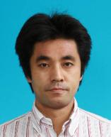
Associate Professor MAKINO Hisao

Dr.Eng., University of Tsukuba, Japan, 1998
Year of birth 1970 Gender Male
Affiliation School of Systems Engineering
Research Institute
Center for Nanotechnology, Research Institute
Materials Design Center, Research Institute
Job titles
Personal web site

Areas of specialization Solid State Physics
Physics of Semiconductor
Thin Film Technology
Laboratory/research office Functional Thin Film Laboratory
Our lab conducts research for the development of materials with new functionality and for innovation in conventional electronic device technology, which is needed to solve current environmental and energy problems and develop a sustainable society. The oxide semiconductor, which is expected to be the foundation next generation electronic material, is considered a new functional material, because of its various useful physical properties. In this laboratory, we are controlling the physical properties of the oxide thin films and are aiming at improvement of the function and creation of new functional devices.
Current reseach topics Atomic Layer Deposition of ZnO Thin Films Properties of Wide Band Gap Semiconductors Application of Transparent Conductive Zinc Oxide Thin Films
Educational background 1998: Doctor, University of Tsukuba, Japan
1993: Bachelor, University of Tsukuba, Japan
Professional background 2014-: Associate Professor, System Engineering. Kochi University of Technology
2007-: Associate Professor, Research Institute, Kochi University of Technology
2005-2007: Assistant professor, Research Institute, Kochi University of Technology
2002-2003: Visiting Researcher, University of Bath
1999-2000: Visiting Researcher, The University of New South Wales
1998-2005: Research Associate, Institute for Materials Research, Tohoku University
Licenses
Academic societies The Japan Society of Applied Physics
The Physical Society of Japan
The Japanese Society of Synchrotron Radiation Research

Courses  * Courses provided in English are shown with (E) mark

Undergraduate school ▼

Fundamentals of Semiconductor Physics
Principles of Semiconductor Devices
Experiments in System Engineering
Graduation Thesis

Graduate school ▼

Advanced Seminar 1
Advanced Seminar 2

Research activities

Research papers ▼

  1. Authors: C. Martin, K.H. Miller, H. Makino, D. Craciun, D. Simeone, V. Craciun
    Title: Optical properties of Ar ions irradiated nanocrystalline ZrC and ZrN thin films
    Journal: Journal of Nuclear Materials, Vol. 488, pp. 16-21
    Year: 2017/05/01
  2. Authors: V. Craciun, D. Craciun, G. Socol, S. Behdad, B. Boesl, C. Himcinschi, H. Makino, M. Socol, D. Simeone
    Title: Investigations of Ar ion irradiation effects on nanocrystalline SiC thin films
    Journal: Applied Surface Science, Vol. 374, pp. 339-345, Elsevier
    Year: 2016/06/30
  3. Authors: Lukman Nulhakim, MAKINO Hisao
    Title: Influence of polarity inversion on the electrical properties of Ga-doped ZnO thin films
    Journal: physica status solidi - Rapid Research Letters, Vol. 10, No. 7, pp. 535-539, Wiley
    Year: 2016
  4. Authors: Lukman Nulhakim, MAKINO Hisao
    Title: Change of scattering mechanism and annealing out of defects on Ga-doped ZnO films deposited by radio-frequency magnetron sputtering
    Journal: Journal of Applied Physics, Vol. 119, p. 235302
    Year: 2016
  5. Authors: NOMOTO Junichi, MAKINO Hisao, YAMAMOTO Tetsuya
    Title: High-Hall-Mobility Al-Doped ZnO Films Having Textured Polycrystalline Structure with a Well-Defined (0001) Orientation
    Journal: Nanoscale Research Letters, Vol. 11, pp. 320-1-320-8, Springer Open
    Year: 2016
  6. Authors: Lukman Nulhakim, MAKINO Hisao
    Title: Control of microstructure by using self-buffer layer and its effects on properties of Ga-doped ZnO thin films deposited by radio frequency magnetron sputtering
    Journal: Thin Solid Films, Vol. 615, pp. 158-164, Elsevier
    Year: 2016
  7. Authors: NOMOTO Junichi, MAKINO Hisao, YAMAMOTO Tetsuya
    Title: Limiting factors of carrier concentration and transport of polycrystalline Ga-doped ZnO films deposited by ion plating with dc arc discharge
    Journal: Thin Solid Films, Vol. 601, pp. 13-17, ELSEVIER
    Year: 2016
  8. Authors: NOMOTO,Junichi, MAKINO, Hisao, YAMAMOTO, Tetsuya
    Title: Carrier mobility of highly transparent conductive Al-doped ZnO polycrystalline films deposited by radio-frequency, direct-current, and radio-frequency-superimposed direct-current magnetron sputtering: Grain boundary effect and scattering in the grain bulk
    Journal: Journal of Applied Physics, Vol. 117, pp. 045304-1-045304-9, AIP Publishing
    Year: 2015/01/23
  9. Authors: S. Kishimoto, S. Akamatsu, SONG, Huaping, NOMOTO,Junichi, MAKINO, Hisao, YAMAMOTO, Tetsuya
    Title: Carbon monoxide gas sensing properties of Ga-doped ZnO film grown by ion plating with DC arc discharge
    Journal: J. Sens. Sens. Syst., Vol. 3, pp. 331-334
    Year: 2014/12
  10. Authors: MAKINO, Hisao, SONG, Huaping, YAMAMOTO, Tetsuya
    Title: Influences of oxygen gas flow rate on electrical properties of Ga-doped ZnO thin films deposited on glass and sapphire substrates
    Journal: Thin Solid Films, Vol. 559, pp. 78-82, Elsevier
    Year: 2014/05
  11. Authors: SONG, Huaping, NOMOTO,Junichi, MAKINO, Hisao, YAMAMOTO, Tetsuya
    Title: Highly moisture resistant Ga-doped ZnO films with textured surface for thin-film solar cells with indium codoping fabricated by ion plating with direct-current arc discharge
    Journal: Jpn. J. Appl. Phys., Vol. 53, pp. 05FJ04-1-05FJ04-5
    Year: 2014/05
  12. Authors: T. Terasako, Y. Ogura, S. Fujimoto, SONG, Huaping, MAKINO, Hisao, M. Yagi, S. Shirakata, YAMAMOTO, Tetsuya
    Title: Carrier transport and photoluminescence properties of Ga-doped ZnO films grown by ion-plating and by atmospheric-pressure CVD
    Journal: Thin Solid Films, Vol. 549, pp. 12-17, Elsevier
    Year: 2013/12
  13. Authors: T. Terasako, SONG, Huaping, MAKINO, Hisao, S. Shirakata, YAMAMOTO, Tetsuya
    Title: Temperature dependence of electrical properties of Ga-doped ZnO films deposited by ion plating with DC arc discharge
    Journal: Thin Solid Films, Vol. 528, pp. 19-25, Elsevier
    Year: 2013/01
  14. Authors: YAMAMOTO, Naoki, Makino, Hisao, Yamamoto, Tetsuya
    Title: Young’s Modulus and Coefficient of Linear Thermal Expansion of ZnO Conductive and Transparent Ultra-Thin Films
    Journal: Advances in Materials Science and Engineering, Vol. 2011
    Year: 2011/10
  15. Authors: YAMAMOTO, Naoki, Makino, Hisao, Osone, Satoshi, Ujihara, Akira, Ito, Takahiro, Hokari, Hitoshi, Maruyama, Taketo, Yamamoto, Tetsuya
    Title: Development of Ga-doped ZnO Transparent Electrodes for Liquid Crystal Display Panels
    Journal: Thin Solid Films
    Year: 2011
  16. Authors: H. Makino, T. Yamada, N. Yamamoto, T. Yamamoto
    Title: Effects of the O2 flow rate and post-deposition thermal annealing on the optical absorption spectra of Ga-doped ZnO films
    Journal: Thin Solid Films, Vol. 519, No. 5, pp. 1521-1524
    Year: 2010/12
  17. Authors: T. Yamada, H. Makino,, N. Yamamoto, T. Yamamoto
    Title: Ingrain and grain boundary scattering effects on electron mobility of transparent conducting polycrystalline Ga-doped ZnO films
    Journal: J. Appl. Phys., Vol. 107, p. 123534
    Year: 2010
  18. Authors: YAMAMOTO, Naoki, Yamada Takahiro, Makino, Hisao, Yamamoto, Tetsuya
    Title: Heat Resistance of Ga-Doped ZnO Thin Films for Application as Transparent Electrodes in Liquid Crystal Displays
    Journal: J. Electrochem. Soc., Vol. 157, pp. J13-J20
    Year: 2010
  19. Authors: H. Makino, N. Yamamoto, A. Miyake, T. Yamada, Y. Hirashima, H. Iwaoka, T. Itoh, H. Hokari, H. Aoki, T. Yamamoto
    Title: Influence of thermal annealing on electrical and optical properties of Ga-doped ZnO thin film
    Journal: Thin Solid Films, Vol. 518, No. 5, pp. 1386-1389
    Year: 2009/12
  20. Authors: H. Makino, S. Kishimoto, A. Miyake, T. Yamada, N. Yamamoto, T. Yamamoto
    Title: Influence of substrate temperature and Zn-precursors on atomic layer deposition of polycrystalline ZnO films on glass, H. Makino, A. Miyake, T. Yamada, N. Yamamoto, T. Yamamoto,
    Journal: Thin Solid Films, Vol. 517, p. 3138
    Year: 2009
  21. Authors: H. Makino, S. Kishimoto, A. Miyake, T. Yamada, N. Yamamoto, T. Yamamoto
    Title: Effects of surface pretreatment on growth of ZnO on glass substrate
    Journal: phys. stat. sol. (a), Vol. 205, No. 8, pp. 1971-1974
    Year: 2008/07
  22. Authors: Tetsuya Yamamoto, Takahiro Yamada, Aki Miyake, Toshiyuki Morizane, Tooru Arimitsu, Hisao Makino, Naoki Yamamoto
    Title: Properties of Transparent Conductive Ga-Doped ZnO Films on Glass, PMMA and COP Substrates
    Journal: Invited Paper, IEICE TRANSACTIONS on Electronics, Vol. E91-C, No. 10, pp. 1547-1553
    Year: 2008
  23. Authors: YAMAMOTO, Naoki, Yamada, Takahiro, Miyake, Aki, Makino, Hisao, Kishimoto, Seiichi, Yamamoto, Tetsuya
    Title: Relationship between Residual stress and Crystallographic Structure in Ga-doped ZnO Film
    Journal: J. Electrochem. Soc., Vol. 155, No. 9, pp. J221-J225
    Year: 2008
  24. Authors: T. Yamada, A. Miyake, S. Kishimoto, H. Makino, N. Yamamoto, T. Yamamoto
    Title: Low resistivity Ga-doped ZnO thin films of less than 100 nm thickness prepared by ion plating with direct current arc discharge
    Journal: Appl. Phys. Lett., Vol. 91, p. 051915
    Year: 2007
  25. Authors: Seiichi Kishimoto, Takahiro Yamada, Keigo Ikeda, Hisao Makino, Tetsuya Yamamoto
    Title: Effects of oxygen partial pressure on film growth and electrical properties of undoped ZnO films with thichness below 100nm
    Journal: Surface & Coatings Technology, Vol. 201, pp. 4000-4003
    Year: 2006
  26. Authors: H. Makino, T. Goto, T. Yao, G. A. Mousdis, G. C. Papavassiliou
    Title: Induced absorption and spontaneous emission due to biexciton in two-dimensional semiconductor (CH3C6H4CH2NH3)2PbBr4 single crysta
    Journal: J. Lumines, Vol. 112, No. 54-57
    Year: 2005
  27. Authors: Hisao Makino, J. J. Kim, P. P. Chen, M. W. Cho, Takafumi Yao
    Title: Making ferromagnetic semiconductors out of III-V nitride semiconductors
    Journal: Proc. SPIE Int. Soc. Opt. Eng., Vol. 5774, p. 11
    Year: 2004
  28. Authors: J. J. Kim, H. Makino, K. Kobayashi, Y. Takata, T. Yamamoto, T. Hanada, M. W. Cho, E. Ikenaga, M. Yabashi, D. Miwa, Y. Nishino, K. Tamasaku, T. Ishikawa, S. Shin, T. Yao
    Title: Hybridization of Cr 3d-N 2p-Ga 4s in the wide band gap diluted magnetic semiconductor Ga1-xCrxN
    Journal: Phys. Rev. B, Vol. 70, p. 161315(R)
    Year: 2004
  29. Authors: N. Taghavinia, H. Makino, T. Yao
    Title: Enhancement of Mn luminescence in ZnS:Mn multi-quantum-well structures
    Journal: Appl. Phys. Lett., Vol. 83, p. 4616
    Year: 2003
  30. Authors: K. Godo, H. Makino, M. W. Cho, J. H. Chang, Y. Yamazaki, T. Yao, M. Y. Shen, T. Goto
    Title: Composition dependence of the energy gap of Zn1-x-yMgxBeySe quaternary alloys nearly lattice matched to GaAs
    Journal: Appl. Phys. Lett., Vol. 79, pp. 4168-4170
    Year: 2001
  31. Authors: H. Makino, H. Sasaki, J.H. Chang, T. Yao
    Title: Raman investigation of Zn1-x-yMgxSe1-yTey quaternary alloys grown by molecular beam epitaxy
    Journal: J. Cryst. Growth, Vol. 214/215, pp. 359-363
    Year: 2000
  32. Authors: H. Makino, I. H. Inoue, M. J. Rozenberg, I. Hase, Y. Aiura, S. Onari
    Title: Bandwidth control in a perovskite-type 3d1-correlated metal Ca1-xSrxVO3. II. Optical spectroscopy
    Journal: Phys. Rev. B, Vol. 58, pp. 4384-4393
    Year: 1998

Keynote lectures ▼

Invited lectures ▼

Notable projects ▼

Awards ▼

Patents ▼

Grants-in-Aid for Scientific Research from the Japanese government ▼

  1. Project title: Control of crystal orientation and acceptor doping properties on polycrystalline zinc oxide thin films
    Category: Grant-in-Aid for Scientific Research(C)
    Project number: 
    Project period: 2011/04-2014/03
    Total budget amount: 5,330,000 yen
    Keywords: 

Competitive research funds ▼

Social activities

Committee roles ▼

Published books ▼