- TOP
- Research
- Research Institute
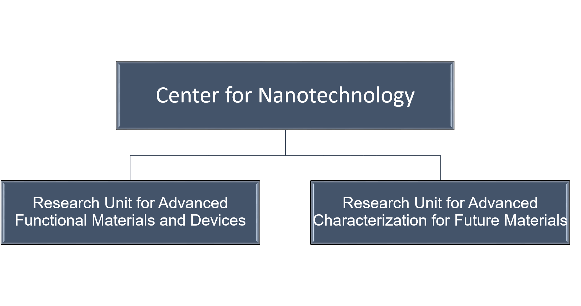
- Center for Nanotechnology
Center for Nanotechnology

Toward Designing Sustainable Societies
The Center for Nanotechnology was established in April 2014 within the Research Institute, after the reorganization of the Institute for Nanotechnology, which originally opened in 2011. In April 2020, with the aim of furthering development of nanotechnology research, two specific fields were placed under the center: Advanced Functional Materials and Devices and Advanced Characterization for Future Materials.
Nanotechnology, an advanced research field involving a wide range of disciplines, occupies a prominent position among Japan's national research strategies.
KUT has been generating a large number of research achievements and outcomes which are important keys to the development of nanotechnology in the fields of material science and electronic engineering.
As a result, the Center for Nanotechnology has been leading nanotechnology research in areas such as the development of nanomaterial synthesis methods, physical property evaluation and the development of device applications.
This contribution is large, and is of significance not only to Kochi Prefecture but to the whole country in terms of industrial promotion.
Research related to nanotechnology tends to need large-scale facilities such as a cleanroom and expensive analytical devices including a transmission electron microscope.
Rather than owning and operating such facilities or equipment in individual labs, KUT has been promoting strategic research material investment as a catalyst for new research themes through multidisciplinary and organizational research projects.
This strategy has led to various joint research projects and the acquisition of competitive research funds, and the educational impact is growing in significance as many students utilize these facilities and equipment every year.
The Center for Nanotechnology is aiming at further research promotion and development in the future.
Research Unit for Advanced Functional Materials and Devices
Objectives for the unit
This field focuses on 1) the creation of quantum functional materials and devices through application of metal oxide semiconductor nanomaterial science; 2) the creation of flexible materials and devices through material synthesis and device construction on a variety of curved surfaces; and 3) the creation of neuromorphic elements using ultra-sensitive sensors and nanotube materials by controlling nanomaterials and their structures, contributing to the development new fields within nanotechnology through collaboration between faculty members specializing in the materials and devices fields.
Regarding material synthesis, with the goal of achieving a wide range of techniques for state control of materials ranging from crystalline to amorphous, we will introduce new means of defect evaluation, atom observation and operation, with the long term goal of creating fusion areas and other new areas of study. In addition, using characteristic experimental environments such as clean rooms, hard X-ray photoelectron spectroscopy, and probe microscopy, we will carry out concerted efforts ranging from the synthesis and evaluation of new materials to device verification, with the goal of enhancing the practice of new education and research.
Major research topics
Creation of quantum functional materials and devices
Within this research theme, we aim to create quantum functional materials and devices by broad-range control of crystal structure. Important materials used will include 1) amorphous materials, e.g. the hydrogenated metal oxide material; and 2) crystalline material, e.g. high-quality metal oxide single crystal material created using the mist vapor phase epitaxy method, an atmospheric pressure film formation method. We will work on the realization of quantum effects in a wide range of crystal structure regions ranging from single crystal to amorphous.
Creation of new flexible materials and devices
Within this research theme, aiming at material synthesis and device construction on a variety of curved surfaces, we will work to create unprecedented flexible materials and devices, such as 1) thin film synthesis technology for tube inner walls and surfaces with varied curvature, for which film formation has been difficult until now; and 2) the realization of high-performance devices on flexible materials such as plastic, by means of material synthesis at lower temperatures.
Creation of ultra-sensitive sensors and neuromorphic elements
Within this research theme, we will work to create new material and device technologies, such as ultra-sensitive sensing devices, by controlling oxide semiconductor nanostructures and neuromorphic elements using nanotube materials.
Research Unit for Advanced Characterization for Future Materials
Objectives for the unit
Since it opened in April 1997, Kochi University of Technology, with the high aspiration of "Making KUT a world class university through the pursuit of unique excellence," has rapidly pursued an education system with advanced aspects such as a quota system, and has been an agile, cutting edge player. To that end, it is necessary for KUT to have a strong commitment to gathering world-class researchers to produce world-class research results in an excellent research environment, and to creating a "visible research center
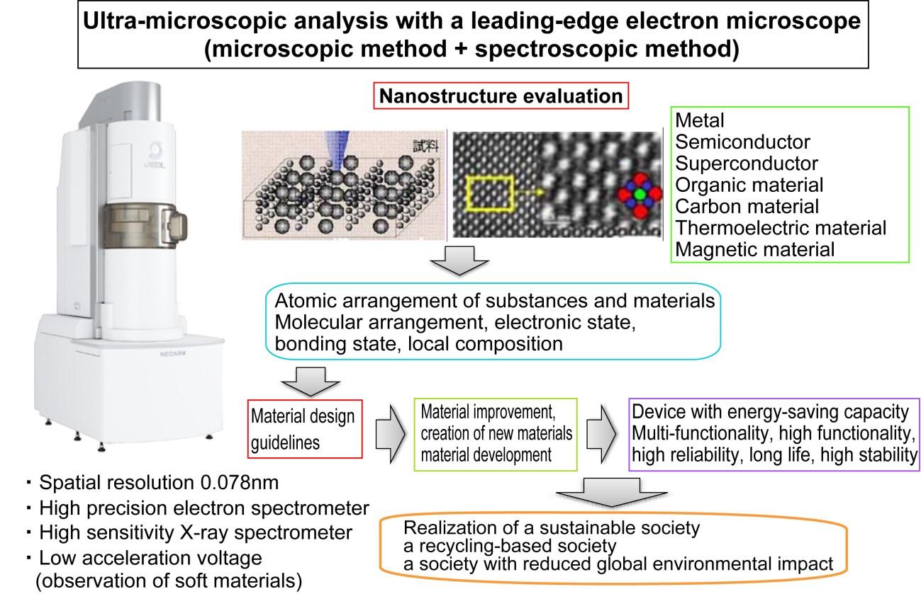
For the strong pursuit of education and research and development at this university, it is essential to acquire a full and accurate grasp of the structures and crystalline architecture (or electronic structures) of a wide variety of substances. The state-of-the-art device for achieving this purpose most efficiently is the transmission electron microscope. In fiscal 2020, KUT will install a transmission electron microscope, including general-purpose elements that have contributed to great strides in spatial and energy resolution; this will greatly enhance KUT's potential for research and development centering on atomic and molecular materials. We will build a user-friendly nano-analysis base in Kochi Prefecture, to accommodate this electron microscope system with multifaceted analysis functions, thus contributing to the nano-science capabilities in the Shikoku region.
Goals of the unit
(1) To make cutting-edge microscopy equipment and technology centered on electron microscopes available on campus, so as to empower students and faculty members to contribute to the advancement of educational research at Kochi University of Technology.
(2) To achieve, through applied research aimed at meeting the needs of society, cutting-edge research results in areas including nanomaterials, biotechnology, environment and energy--all directly linked to Japan's national strategies for science and technology.
(3) To establish an international core research center for electron microscopy and its application fields, and to enhance KUT facilities and equipment so as to support research exchanges both within and outside Japan.
(4) To promote industry-academia-government collaboration and cooperation in electron microscopy and its application fields. In particular, in the fields of nanotechnology and materials, research agendas will be set and their pursuit will be promoted in collaboration with the local community.
(5) To strengthen global collaboration in electron microscopy and its application fields, and promote exchanges and collaboration with industry-academia-government in other Asian countries.
(6) To strengthen the related research network on a global scale and to build a collaborative system with Asian universities, research institutes and industry.
Major research topics
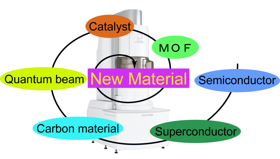
Given the game changing potential of the discovery and creation of new substances, we aim to apply electron microscopy to the creation of new substances based on nano-control.
(1) Creation of new catalytic materials by controlling nanostructures
(2) Realization of precision design of crystal structures of metal organic frameworks (MOF) and development of the functionality of those frameworks
(3) Fabrication of new semiconductor materials based on non-equilibrium processes (quantum beam and plasma); and development of applications of those materials
(4) Creation of new nano-carbon materials
(5) Discovery of a new high-temperature superconductor